

Time-Of-Flight Neutron Depth Profiling (TOF NDP) at Penn State Breazeale Nuclear Reactor
| Participants: | Kenan Ünlü, Professor of Mechanical and Nuclear Engineering |
| S. M. Çetiner, Ph.D Student of Mechanical and Nuclear Engineering | |
| Services Provided: | Neutron Beam Laboratory |
| Sponsors: | U.S. Department of Energy, under Nuclear Engineering Education Research (NEER) grant |
Introduction
Neutron Depth Profiling (NDP) is a near-surface analysis technique to measure the spatial distribution of certain isotopes of technological importance in any substrate. The NDP technique was originally developed by Ziegler et al [ 1 , 2 ] in 1972, and later thoroughly investigated by Biersack et al [ 3 ]. The basis of NDP is the irradiation of a sample with thermal or sub-thermal neutrons and the subsequent release of charged particles due to neutron induced exoergic charged particle reactions. Neutrons interact with the nuclei of isotopes 10B, 3He, 6Li, 7Be and 22Na etc, and release mono energetic charged particles, e.g. alpha particles or protons, and recoil atoms. Table 1 gives a detailed listing of other relevant NDP reactions.
The charged particles travel outward and lose energy by numerous interactions with the electrons of the host matrix. Measuring the residual energy of the charged particles or recoil atoms and knowing the stopping power of the host matrix allow for the determination of the depth profile of the isotope of interest inside the matrix. The reader is recommended to refer K. Ünlü et al [ 4 - 8 ] for a comprehensive discussion.
Principles of the TOF NDP
In conventional NDP, the residual energies of charged particles are measured directly by using silicon surface barrier, PIPS, or silicon PIN photodiode detectors. However, because of the physics, there is an error inherent in the measurement process. Conventional semiconductor detectors employ a dead layer at the entrance of the active area. The energy transfer in this layer brings statistical uncertainty to the energies of the charged particles, which are created at single energies and only have a distribution because of the thickness of the material of interest.
In TOF NDP, however, the residual energies of charged particles are not measured directly, but instead it is deduced based on the time-of-flight measurement spectrum.
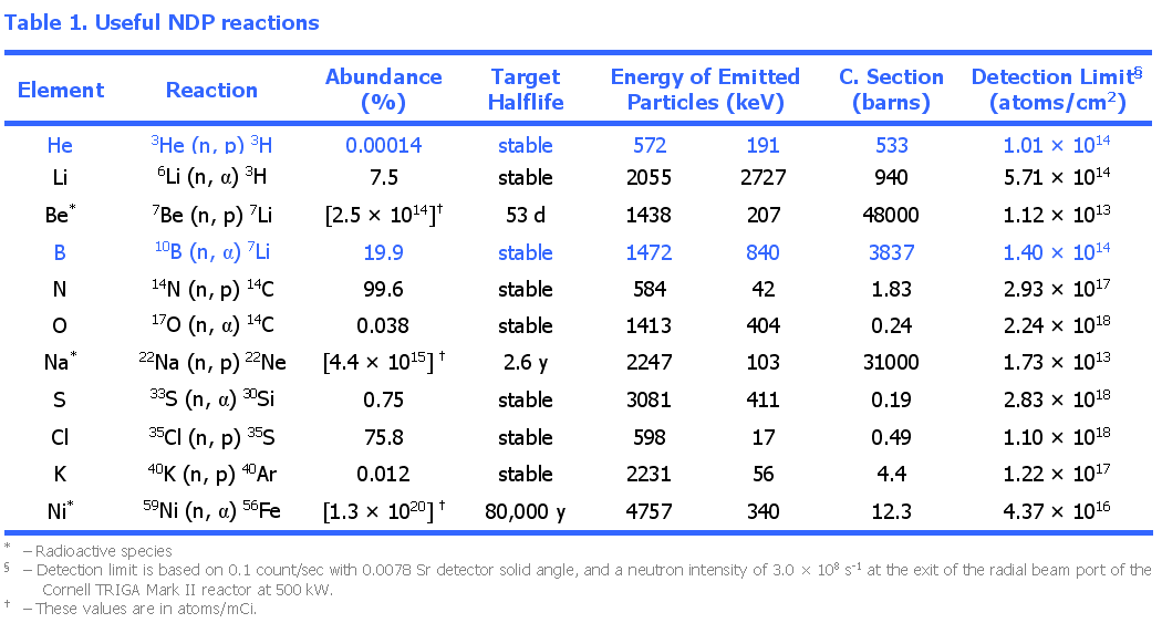
The time-of-flight information of each particle is obtained from the time difference between the pulses generated by the start and stop detectors. The start detector is triggered by electrons that are sprayed out of the surface of the sample as a charge particle leaves the surface. This is almost a spontaneous process. However, these electrons are ejected from the surface with very small energies and therefore they need to be accelerated for efficient signal processing.
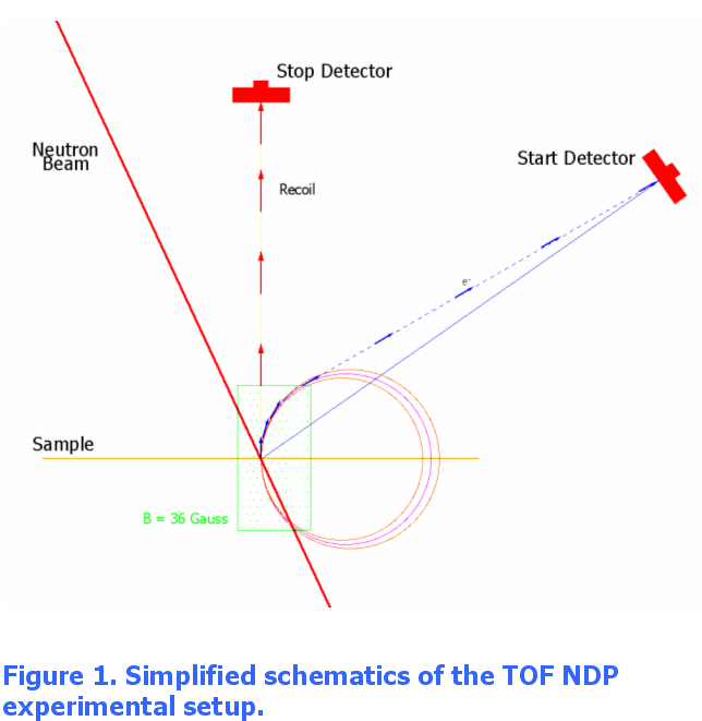
An electrical field on the path of the particles accelerates electrons. The field is created between the sample plate and a specially manufactured sieve as seen on Figure 2. The micro-mesh structure on the sieves behaves both as a permeable anode surface and filter that eliminates electrons that move off the line of sight. The potential difference between the sample plate and the sieve, which we call “acceleration region”, causes an electron to achieve very high velocities because of its miniscule mass. A conceptual schematics of the TOF NDP setup is shown in Figure 1.
An electromagnet steers electrons onto the start detector. Since the mass of electron is small, the amount of magnetic field required is also very limited. This allows for selective particle transfer, i.e. focusing electrons onto the start detector and letting recoils, proton or alphas go directly at the stop detector.
The signals generated by the two multi-channel plate (MCP) detectors have very high precision timing information. These signals are fed into two fast-timing amplifiers that provide time discrimination. Originally, the signals that come out of the MCP’s are current pulses. The output of the time discriminator becomes voltage pulses and also reshaped in order to make them compatible with the time-of-flight time analyzer.
Time analyzer is the central part of the time-of-flight analysis. It behaves like a multi-channel analyzer in time domain, where varying time differences constitute the time span of the spectrum. In order to do that, the time difference between the two signals is discretized. If the time analyzer reads a signal that falls into a discrete time channel, it increases the counter value associated with this particular channel by one. This way, a spectral distribution is created where the left-hand side of the spectrum represents the smallest time difference and hence the fastest traveling recoils.
Preparing the Test Sample for Initial Experimentation
Time-of-flight test system will ultimately be used in front of the reactor beam for industrial test samples, particularly from the semiconductor industry. However, preliminary experimentation with the system and at the earlier stages of – will require an adaptation process. In order to avoid unnecessary occupation of the nuclear reactor time, we decided to proceed with a test sample that will give a detectable depth profile to test the integrity and reliability of the setup. Once we become confident that the depth profile obtained by the time-of-flight setup is within the limits of expectations, we then plan to start to repeat the NDP experiments that were done with conventional methods.
The test sample will be a monoenergetic alpha source. Polonium-210 is an isotope that emits alpha particles single energy and not followed by any additional radiation. This alleviates the analysis of signals by the electronic circuitry.
In order to get a depth distribution that will emphasize the functionality of the system, we decided to do a polonium-210 surface implantation on a thin silver foil. The electrochemistry between silver and polonium makes it possible to do surface implantation without employing sophisticated techniques. The affinity of silver to polonium forces polonium atoms to diffuse into a certain depth from the surface, but not get distributed homogeneously. This is done by putting the silver foil into an acidic polonium solution, in this case polonium-210. Because of the surface affinity in silver, polonium spontaneously deposits itself on the surface of the foil creating an alpha emitter depth profile.
Setting up the TOF NDP System
Time-of-flight NDP system includes two multi-channel plate detectors (MCP), a vacuum chamber, vacuum pumps, and signal processing electronics.
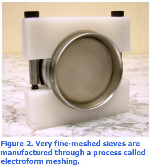
Multi-channel plate (MCP) detectors are very sensitive devices that can easily become defective. We have MCP detectors that are high-precision that were purchased from Hamamatsu . However, we decided to use MCP’s that have manufacturing fault but are still functional in order to avoid the expense of renewing the equipment. The detectors are provided to us by a professional affiliate of the project. However, the MCP’s that are given to us were bare MCP detectors without the assembly. We designed a modular assembly that can operate with various dimensions of MCP detectors and for high voltage levels. Figure 3 shows the 3D CAD drawing of the design.
We also upgraded the PC interface of the time analyzer from an ISA-compatible card to a PCI-compatible card. This gave us the flexibility of using more up-to-date computers and operating systems.
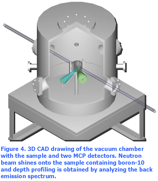
Figure 4 shows a 3D CAD drawing of the vacuum chamber, two MCP detectors and the neutron beam. The drawing is a downscaled representation of the actual vacuum chamber.
The neutron beam enters the chamber through one of the thin aluminum windows and shine on the sample. The neutrons in the beam interact with boron-10 atoms and create alpha and lithium particles. The charged particles are emitted isotropically with respect to the original location of the isotope. From the back emission of recoils and electrons that are ejected from the surface along with recoils, we get the time-of-flight spectra of particles, as explained in more detail in the foregoing section.
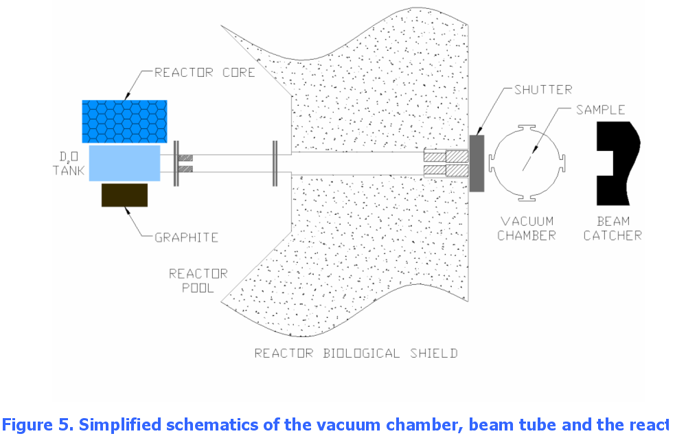
The layout of the test setup in the reactor beam lab is shown in Figure 5. The vacuum chamber is placed in front of one of the beam tubes and is aligned with the neutron beam so that the beam crosses the sample as shown in Figure 4. During the experiment, the reactor core is placed by the D 2O tank. When the reactor reaches the requested power level, the shutter is opened allowing the neutron beam to enter the chamber.
Conclusion and Future Work
As the technology progresses the size of the semiconductor devices go down significantly. The nominal device thickness until couple of generations ago was around 200 nm. Conventional TOF technique provided ample resolution for decent analysis. However, especially with the arrival of ultra-shallow junctions, the technology is now going towards device thicknesses below 90 nm. The resolution obtained by conventional NDP (~ 15-20 nm) is obviously not a statistically adequate represen-tative of such figures. We anticipate a much higher resolution from TOF NDP, less than 5 nm, and this will make it possible to detect isotope profiles of thicknesses less than 100 nm.
Acknowledgement
This project is sponsored by U.S. Department of Energy under Nuclear Engineering Education Research (NEER) grant DE-FG07-00ID-13921.
References
- J. F. Ziegler, G. W. Cole, J. E. E. Baglin , J. Appl. Phys., v. 43 (1972), p. 3809.
- W. K. Chu, V. L. Moruzzi, J. F. Ziegler, J. Appl. Phys., v. 46, No. 7 (1975), pp. 2817-2820.
- J. P. Biersack, D. Fink, R. Henkelmann, K. Müller, Nuc. Inst. Meth., v. 149 (1978), pp. 93-97.
- K. Ünlü and B.W. Wehring, Nucl. Instr. And Meth. Phys. Res. A, v. 353, (1994) p. 402.
- K. Ünlü and D. H. Vincent, "Helium-3 behavior in some Nickel-based Amorphous Alloys," Nuclear Science and Engineering, v. 110, No. 4, April 1992.
- K. Ünlü, M. Saglam, B. W. Wehring, “ 3He and 10B Concentration and Depth Measurements in Alloys and Semiconductors using NDP,” Nucl. Instr. and Meth. in Phys. Res. A, v. 422 (1999) pp. 885-890.
- K. Ünlü et al., IEEE Proc. 11 th Int. Conf. on Ion Imp. Tech., v. 1, 1996, p. 575.
- S. M. Cetiner, K. Ünlü, R. G. Downing, 11 th Int. Conf. on Modern Trends in Activation Analysis, Universi ty of Surrey, Gilford, UK, 2004 (Proceeding will be published in Journal of Radioanalytical and Nuclear Chemistry).
