Neutron Depth Profiling (NDP)
Neutron Depth Profiling (NDP) is a near surface analysis technique to measure nondestructively the concentration versus depth distributions of several isotopes of technological importance in any substrate. The NDP technique was originally developed by Ziegler et al. [1] in 1972, and later thoroughly investigated by Biersack et al. [2,3]. The basis of NDP is the irradiation of a sample with thermal or subthermal neutrons and the subsequent release of charged particles due to neutron induced exoergic charged particle reactions. A schematic of the NDP set-up is given in Figure 1 . Neutrons interact with the nuclei of isotopes 10 B, 3 He, 6 Li, 7 Be and 22 Na etc., and release monoenergetic charged particles, e.g. alpha particles or protons, and recoil atoms. These particles travel outward and lose energy by numerous interactions with the electrons of the host matrix. Measuring the residual energy of the charged particles or recoil atoms and knowing the stopping power of the host matrix allows for the determination of the depth profile of the isotope of interest inside the matrix. A more detailed description of this process is given in reference [4] and possibly useful NDP reactions are given in Table 1 .
The importance of NDP in materials research has been the primary motivation for the development of the Penn State University, Neutron Depth Profiling Facility (PSU-NDP). An important application of PSU-NDP will be the measurement of boron profiles in borophosphosilicate glass (BPSG) samples and 10 B implanted silicon wafers for the semiconductor industry. The 3 He concentration depth profiles in alloys will be measured using PSU-NDP to study possible degradation effects of prolonged alpha irradiation. Some applications of the NDP technique are discussed below and previously measured results are given. Future improvements of the NDP method are also discussed.
Applications of NDP
* He-3 in alloys
The radiation damage in alloys due to 3 He implantation is a problem that can be investigated by using the NDP technique. Helium can modify materials properties because, when introduced into materials, it tends to nucleate as small gas clusters in lattice defects. If the helium fluence is increased, the small gas clusters combine and form gas bubbles. Gas bubbles may recombine and create a pressurized cavity beneath the material surface. When the pressure of the cavity is high enough, it can form blisters and the rupturing of these blisters causes surface flaking or exfoliation. Pressurized helium gas bubbles inside materials may also cause cracks and crack propagation into the bulk which can compromise the structural integrity of materials. The shape of the depth profile gives information about possible microstructural changes occurring in an alloy. For example, the differences in spatial distribution of implanted helium in the near surface region and across interfacial boundaries can significantly affect the helium release phenomena described above.
When a thermal neutron beam strikes the sample containing 3 He the 3 He(n,p) 3 H reaction, with a thermal neutron cross-section of 5330 barns, takes place and is used to obtain the helium depth profile data. From the NDP energy spectrum data the channel numbers are converted to a projected depth using the energy calibration and counts are converted to 3 He concentrations using a reference dose sample. A sample NDP profile is shown in Figure 2 .
The samples that are analyzed with NDP are subsequently observed using Transmission Electron Microscopy and Scanning Electron Microscopy for surface morphology and microstructural changes. A correlation between depth profile and microstructural and surface morphology changes will be obtained as a result of this investigation.
* B-10 in Microelectronics materials
The Application of NDP in the field of microelectronics materials has been an important topic due to the extensive use of boron in semiconductor device fabrication. Some of the more important applications related to semiconductors are:
-- Study of boron distributions in semiconductor materials as a function of wafer treatment.
-- Investigation of boron transport in semiconductor materials, especially across oxide surfaces.
-- Study of boron concentration in microelectronics passive layers as it affects melting temperatures.
-- Study of boron doses of semiconductor materials for dose calibration of commercial ion implant systems.
The PSU-NDP facility will be used routinely for measurement of boron profiles in borophosphosilicate glass (BPSG) which is used as an insulating layer on high density integrated circuits. The thickness of the boron layer in BPSG is an important factor in the production of multilayer circuits. A more detailed description of this application and results can be found in reference [5].
Ion implantation is the most frequent and widely practiced method of doping Si during semiconductor device fabrication. The typical fabrication plant has a series of ion implanters set up to introduce a dopant like boron. The dose of these dopants need to be within a limited tolerance and desired distribution profile in order for reliable device performance. Another important issue is that these multiple implanters must provide the same dose/profile over a period of time in order to yield consistent products. The accurate characterization of the implanted dose is therefore very important. Normally, Secondary Ion Mass Spectroscopy (SIMS) is used to measure the dose and profile. SIMS however is not quantitative without a reliable standard of known dose and profile. NDP provides such a standard for SIMS. Since it is nondestructive the same samples can be subsequently analyzed in SIMS and a cross calibration between the two techniques can be established. Another feature of NDP is that the presence of an interface does not arbitrarily modify the profile like in SIMS. This is due to the insensitivity of neutrons to a matrix or interface. Thus, a profile obtained by NDP can help to resolve or interpret artifacts that might be present in the SIMS measurement.
Figure 3 shows a full spectrum of particles that are emitted by the 10 B(n,alpha) 7 Li reaction for a 120 keV boron-10 implanted silicon wafer at a total dose of 2.0 x 10 16 atoms/cm 2 . A depth versus concentration profile is determined from this spectrum by converting the channel numbers into energies and then calculating the depth for these energies using the characteristic stopping power of the Si wafer. The resulting profile for the boron-10 implanted silicon wafer is shown in Figure 4 .
The corresponding SIMS measurement and calculated depth profile from theoretically predicted distribution (Transfer of Ions in Matter - TRIM) is also shown in the figure. From the concentration profile the total amount of boron-10 in the sample is obtained. The implanted dose was 2 x 10 16 per cm 2 and our measured value is (2.08+ 0.02) x 10 16 per cm 2 . The error is based on the counting statistics only. The profile obtained from the University of Texas at Austin NDP (UT-NDP) and SIMS is in good agreement while the TRIM profile deviated from both towards the deeper depth. A portion of the difference is due to broadening of the rear sides of the measured profiles caused by depth resolution. The NDP depth resolution is due both from electronic straggling and inherited detector resolution. The depth resolution of the UT-NDP facility in its current setup is about 20 nm. Off angle measurements can be made to achieve a resolution of about 10-15 nm. The resolution of the NDP facilities is mainly dependent on the characteristics of the surface-barrier detector that is used.
An important problem that faces the semiconductor industry for the next generation of microprocessor manufacturing is the arrival of shallow junction' devices. The dopants of these devices will be implanted at very low energy and a total depth of ~20 nm. The accurate determination of the dopant depth profiles is of prime interest. The use of SIMS for shallow junction' profiles is inadequate. A variation of the traditional NDP method called Time of Flight NDP (TOF-NDP) may fill this need. This is due to the fact that time-of-flight techniques have generally superior resolution compared to energy measurements made by surface barrier detectors. A TOF-NDP facility is currently being developed at Penn State University. Please contact Prof. Kenan Ünlü at RSEC for details.
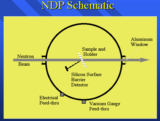
Figure 1.

Table 1.
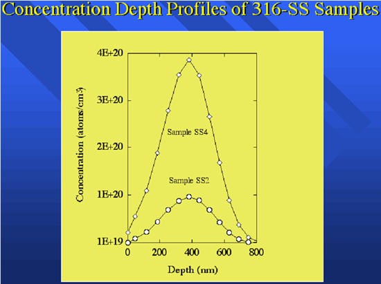
Figure 2.
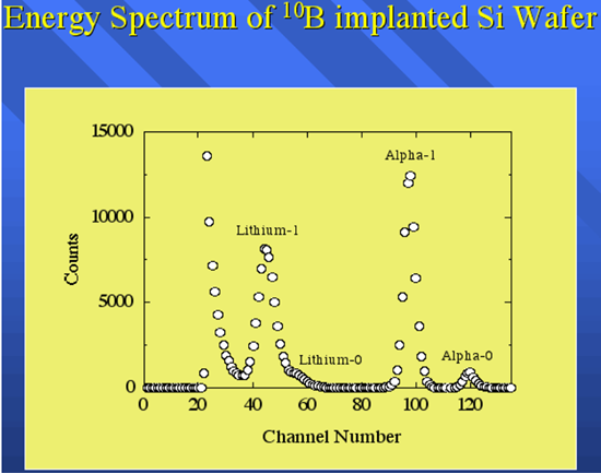
Figure 3.

Figure 4.
References
[1] J.F. Ziegler, G.W. Cole, and J.E.E. Baglin, J. Appl. Phys., Vol. 43 (1972) 3809.
[2] J. P. Biersack, D. Fink, in S. Datz, B. R. Appleton, C. D. Moak, (Eds), Atomic Collisions in Solids, (Plenum Press, New York, 1975) p. 737.
[3] D. Fink, J.P. Biersack, H. Liebl, in H. Ryssel, H. Glawischnig (Eds), Ion implantation: Equipment and Techniques, (Springer-Verlag, Berlin, 1983) p. 318.
[4] K. Ünlü and B.W. Wehring, Nucl. Instr. And Meth. Phys. Res., A, 353, (1994) 402.
[5] K. Ünlü et al., IEEE Proc. of the 11th Int'l Conf. on Ion Imp. Tech., 1 (1996) 575.
|
|
|